- 您现在的位置:买卖IC网 > Sheet目录3876 > PIC18F14K50-I/SS (Microchip Technology)IC PIC MCU FLASH 8KX16 20-SSOP
2010 Microchip Technology Inc.
Preliminary
DS41350E-page 121
PIC18F/LF1XK50
14.4
PWM (Enhanced Mode)
The Enhanced PWM Mode can generate a PWM signal
on up to four different output pins with up to 10-bits of
resolution. It can do this through four different PWM
output modes:
Single PWM
Half-Bridge PWM
Full-Bridge PWM, Forward mode
Full-Bridge PWM, Reverse mode
To select an Enhanced PWM mode, the P1M bits of the
CCP1CON register must be set appropriately.
The PWM outputs are multiplexed with I/O pins and are
designated P1A, P1B, P1C and P1D. The polarity of the
PWM pins is configurable and is selected by setting the
CCP1M bits in the CCP1CON register appropriately.
Table 14-1 shows the pin assignments for each
Enhanced PWM mode.
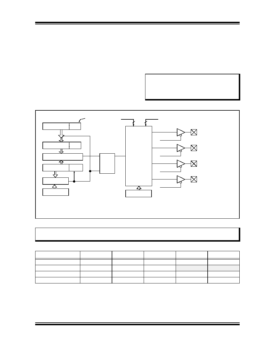
Figure 14-3 shows an example of a simplified block
diagram of the Enhanced PWM module.
FIGURE 14-3:
EXAMPLE SIMPLIFIED BLOCK DIAGRAM OF THE ENHANCED PWM MODE
TABLE 14-2:
EXAMPLE PIN ASSIGNMENTS FOR VARIOUS PWM ENHANCED MODES
Note:
To
prevent
the
generation
of
an
incomplete waveform when the PWM is
first enabled, the ECCP module waits until
the start of a new PWM period before
generating a PWM signal.
CCPR1L
CCPR1H (Slave)
Comparator
TMR2
Comparator
PR2
(1)
RQ
S
Duty Cycle Registers
DC1B<1:0>
Clear Timer2,
toggle PWM pin and
latch duty cycle
Note
1:
The 8-bit timer TMR2 register is concatenated with the 2-bit internal Q clock, or 2 bits of the prescaler to create the 10-bit
time base.
TRIS
CCP1/P1A
TRIS
P1B
TRIS
P1C
TRIS
P1D
Output
Controller
P1M<1:0>
2
CCP1M<3:0>
4
PWM1CON
CCP1/P1A
P1B
P1C
P1D
Note 1: The TRIS register value for each PWM output must be configured appropriately.
2: Any pin not used by an Enhanced PWM mode is available for alternate pin functions.
ECCP Mode
P1M<1:0>
CCP1/P1A
P1B
P1C
P1D
Single
00
Yes(1)
Half-Bridge
10
Yes
No
Full-Bridge, Forward
01
Yes
Full-Bridge, Reverse
11
Yes
Note 1:
Outputs are enabled by pulse steering in Single mode. See Register 14-4.
发布紧急采购,3分钟左右您将得到回复。
相关PDF资料
PIC24F08KL302-I/ML
IC MCU 16BIT 8KB FLASH 28-QFN
PIC24F08KL302-I/MQ
IC MCU 16BIT 8KB FLASH 28-QFN
PIC16LF627A-I/P
IC MCU FLASH 1KX14 EEPROM 18DIP
PIC18F25K20-I/SO
IC PIC MCU FLASH 16KX16 28SOIC
PIC24F08KL301-I/SO
IC MCU 16BIT 8KB FLASH 20-SOIC
PIC24F04KL101-I/P
IC MCU 16BIT 4KB FLASH 20-PDIP
PIC16LC56A-04/SO
IC MCU OTP 1KX12 18SOIC
PIC16LF74-I/PTG
IC MCU FLASH 4KX14 44TQFP
相关代理商/技术参数
PIC18F14K50T-I/SO
功能描述:8位微控制器 -MCU 16KB Flash 768 RAM15 I/O 10-B ADC USB 2.0
RoHS:否 制造商:Silicon Labs 核心:8051 处理器系列:C8051F39x 数据总线宽度:8 bit 最大时钟频率:50 MHz 程序存储器大小:16 KB 数据 RAM 大小:1 KB 片上 ADC:Yes 工作电源电压:1.8 V to 3.6 V 工作温度范围:- 40 C to + 105 C 封装 / 箱体:QFN-20 安装风格:SMD/SMT
PIC18F14K50T-I/SS
功能描述:8位微控制器 -MCU 16KB Flash 768 RAM15 I/O 10-B ADC USB 2.0
RoHS:否 制造商:Silicon Labs 核心:8051 处理器系列:C8051F39x 数据总线宽度:8 bit 最大时钟频率:50 MHz 程序存储器大小:16 KB 数据 RAM 大小:1 KB 片上 ADC:Yes 工作电源电压:1.8 V to 3.6 V 工作温度范围:- 40 C to + 105 C 封装 / 箱体:QFN-20 安装风格:SMD/SMT
PIC18F2220-E/SO
功能描述:8位微控制器 -MCU 4KB 512 RAM 25 I/O RoHS:否 制造商:Silicon Labs 核心:8051 处理器系列:C8051F39x 数据总线宽度:8 bit 最大时钟频率:50 MHz 程序存储器大小:16 KB 数据 RAM 大小:1 KB 片上 ADC:Yes 工作电源电压:1.8 V to 3.6 V 工作温度范围:- 40 C to + 105 C 封装 / 箱体:QFN-20 安装风格:SMD/SMT
PIC18F2220-E/SP
功能描述:8位微控制器 -MCU 4KB 512 RAM 25 I/O RoHS:否 制造商:Silicon Labs 核心:8051 处理器系列:C8051F39x 数据总线宽度:8 bit 最大时钟频率:50 MHz 程序存储器大小:16 KB 数据 RAM 大小:1 KB 片上 ADC:Yes 工作电源电压:1.8 V to 3.6 V 工作温度范围:- 40 C to + 105 C 封装 / 箱体:QFN-20 安装风格:SMD/SMT
PIC18F2220-I/SO
功能描述:8位微控制器 -MCU 4KB 512 RAM 25 I/O RoHS:否 制造商:Silicon Labs 核心:8051 处理器系列:C8051F39x 数据总线宽度:8 bit 最大时钟频率:50 MHz 程序存储器大小:16 KB 数据 RAM 大小:1 KB 片上 ADC:Yes 工作电源电压:1.8 V to 3.6 V 工作温度范围:- 40 C to + 105 C 封装 / 箱体:QFN-20 安装风格:SMD/SMT
PIC18F2220-I/SO
制造商:Microchip Technology Inc 功能描述:IC 8BIT FLASH MCU 18F2220 SOIC28
PIC18F2220-I/SOC03
制造商:Microchip Technology Inc 功能描述:
PIC18F2220-I/SP
功能描述:8位微控制器 -MCU 4KB 512 RAM 25 I/O RoHS:否 制造商:Silicon Labs 核心:8051 处理器系列:C8051F39x 数据总线宽度:8 bit 最大时钟频率:50 MHz 程序存储器大小:16 KB 数据 RAM 大小:1 KB 片上 ADC:Yes 工作电源电压:1.8 V to 3.6 V 工作温度范围:- 40 C to + 105 C 封装 / 箱体:QFN-20 安装风格:SMD/SMT